(Hong Kong)


Product Summary
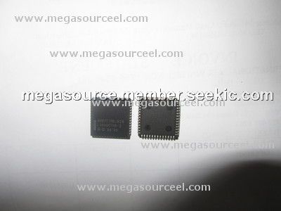
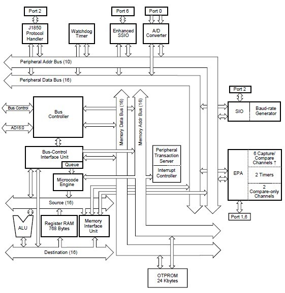
The AN87C196LB20 is a high-performance 16-bit microcontroller with integrated support for the J1850 communication protocol. The AN87C196LB20 is composed of a high-speed core with the following peripherals: an asynchronous/synchronous serial I/O port (8096 compatible) with a dedicated 16-bit baud-rate generator; an additional synchronous serial I/O port with full duplex master/slave transceivers; a six-channel A/D converter with sample and hold; a flexible timer/counter structure with prescaler, cascading, and quadrature capabilities; six modularized, multiplexed high-speed I/O for capture and compare (called event processor array) with 200 ns resolution and double buffered inputs; and a sophisticated prioritized interrupt structure with programmable peripheral transaction server (PTS). The clock doubler circuitry and oscillator output signal enable a 4 MHz resonator to achieve the same internal clock speed as a more costly 8 MHz resonator in previous applications. This AN87C196LB20 circuitry can drive other devices where a separate resonator was required in the past. Another costsavings feature of AN87C196LB20 is the fact that the I/O ports are driven low at reset, avoiding the need for pull-up resistors.
Parametrics
AN87C196LB20 absolute maximum ratings: (1)Storage Temperature: -60℃ to +150℃; (2)Voltage from VPP or EA# to VSS or ANGND: -0.5V to +13.0 V; (3)Voltage from any other pin to VSS or ANGND: -0.5V to +7.0V; (4)Power Dissipation: 0.5 W.
Features
AN87C196LB20 features: (1)20 MHz operation 24 Kbytes of on-chip OTPROM; (2)768 bytes of on-chip register RAM; (3)Register-to-register architecture; (4)Peripheral transactioserver (PTS) with high-speed, microcoded interrupt service routines; (5)Integrated, industry-standard J1850 communicatioprotocol; (6)Six-channel/10-bit A/D with sample and hold; (7)High-speed event processor array; (8)Full-duplex serial I/O port with dedicated baud-rate generator; (9)Enhanced full-duplex, synchronous serial I/O port (SSIO); (10)Programmable 8- or 16-bit external bus; (11)Optional clock doubler with programmable clock output signal; (12)SFR register that indicates the source of the last reset; (13)Desigenhancements for EMI reduction; (14)Oscillator failure detectiocircuitry; (15)Watchdog timer (WDT).
Diagrams
 |
 AN8725FH |
Other |
|
Data Sheet |
Negotiable |
|
||||
|
AN8730SB |
Other |
|
Data Sheet |
Negotiable |
|
||||
|
AN8735NSB |
Other |
|
Data Sheet |
Negotiable |
|
||||
|
AN8737SB |
Other |
|
Data Sheet |
Negotiable |
|
||||
|
AN8746SA |
Other |
|
Data Sheet |
Negotiable |
|
||||
|
AN8771NFH |
Other |
|
Data Sheet |
Negotiable |
|
||||