(Hong Kong)

Product Summary
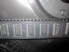
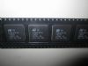
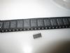
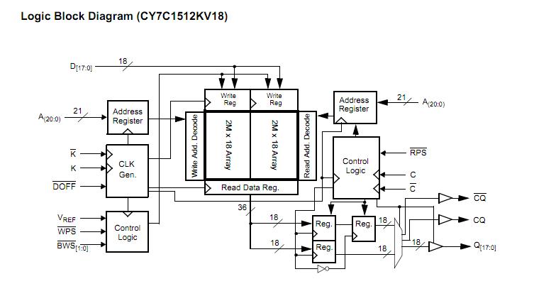
The CY7C1512KV18-250BZC is a 1.8V Synchronous Pipelined SRAM, equipped with QDR-II architecture. QDR-II architecture consists of two separate ports: the read port and the write port to access the memory array. The CY7C1512KV18-250BZC read port has dedicated data outputs ton support read operations and the write port has dedicated data inputs to support write operations.
Parametrics
CY7C1512KV18-250BZC absolute maximum ratings: (1)Storage Temperature:–65 to +150℃; (2)Ambient Temperature with Power Applied: –55 to +125℃; (3)Supply Voltage on VDD Relative to GND:–0.5V to +2.9V; (4)Supply Voltage on VDDQ Relative to GND:–0.5V to +VDD; (5)DC Applied to Outputs in High-Z: –0.5V to VDDQ + 0.5V; (6)DC Input Voltage: –0.5V to VDD + 0.5V; (7)Current into Outputs (LOW): 20 mA; (8)Static Discharge Voltage (MIL-STD-883, M. 3015): > 2001V; (9)Latch up Current: > 200 mA.
Features
CY7C1512KV18-250BZC features: (1)Separate Independent Read and Write Data Ports; (2)333 MHz Clock for High Bandwidth; (3)2-word Burst on all Accesses; (4)Double Data Rate (DDR) Interfaces on both Read and Write Ports (data transferred at 666 MHz) at 333 MHz ; (5)Two Input Clocks (K and K) for precise DDR timing; (6)Two Input Clocks for Output Data (C and C) to minimize Clock Skew and Flight Time mismatches; (7)Echo Clocks (CQ and CQ) simplify Data Capture in High Speed Systems; (8)Single Multiplexed Address Input bus latches Address Inputs for both Read and Write Ports; (9)Separate Port Selects for Depth Expansion; (10)Synchronous internally Self-timed Writes; (11)QDR-II operates with 1.5 Cycle Read Latency when DOFF is asserted HIGH; (12)Operates similar to QDR-I Device with 1 Cycle Read Latency when DOFF is asserted LOW; (13)Full Data Coherency, providing Most Current Data; (14)Core VDD = 1.8V (±0.1V); IO VDDQ = 1.4V to VDD; (15)Offered in both Pb-free and non Pb-free Packages; (16)Variable Drive HSTL Output Buffers; (17)JTAG 1149.1 Compatible Test Access Port; (18)Phase Locked Loop (PLL) for Accurate Data Placement.
Diagrams
| Image | Part No | Mfg | Description |  |
Pricing (USD) |
Quantity | ||||||||
|---|---|---|---|---|---|---|---|---|---|---|---|---|---|---|
 |
 CY7C1512KV18-250BZC |
Cypress Semiconductor |
SRAM 4Mb x 18 250 MHz |
Data Sheet |
|
|
||||||||
 |
CY7C1512KV18-250BZCT |
Cypress Semiconductor |
SRAM 4Mx18 72MB 2.9V |
Data Sheet |
|
|
||||||||