(Hong Kong)


Product Summary
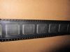
The K4N56163QG-ZC25 is a 256Mb gDDR2 SDRAM chip. It is organized as 4Mbit x 16 I/O 4banks banks device. This synchronous device achieve high speed graphic double-data-rate transfer rates of up to 1000Mb/sec/pin for general applications. The chip K4N56163QG-ZC25 is designed to comply with the following key gDDR2 SDRAM features such as posted CAS with additive latency, write latency read latency - 1, Off-Chip Driver(OCD) impedance adjustment and On Die Termination.
Parametrics
K4N56163QG-ZC25 absolute maximum ratings: (1)VDD Voltage on VDD pin relative to Vss - 1.0 V ~ 2.3 V; (2)VDDQ Voltage on VDDQ pin relative to Vss - 0.5 V ~ 2.3 V; (3)VDDL Voltage on VDDL pin relative to Vss - 0.5 V ~ 2.3 V; (4)VIN, VOUT Voltage on any pin relative to Vss - 0.5 V ~ 2.3 V; (5)TSTG Storage Temperature -55 to +100℃.
Features
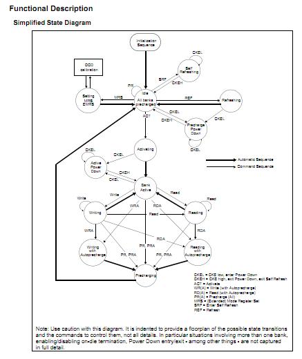
K4N56163QG-ZC25 features: (1)1.8V + 0.1V power supply for device operation; (2)1.8V + 0.1V power supply for I/O interface; (3)4 Banks operation; (4)Posted CAS; (5)Programmable CAS Letency : 4, 5, 6 and 7; (6)Programmable Additive Latency : 0, 1, 2, 3, 4 and 5; (7)Write Latency (WL) = Read Latency (RL) -1; (8)Burst Legth : 4 and 8 (Interleave/nibble sequential); (9)Programmable Sequential/ Interleave Burst Mode.
Diagrams
 |
 K4N56163QF-GC |
Other |
|
Data Sheet |
Negotiable |
|
||||
|
K4N51163QC-ZC |
Other |
|
Data Sheet |
Negotiable |
|
||||