(Hong Kong)


Product Summary
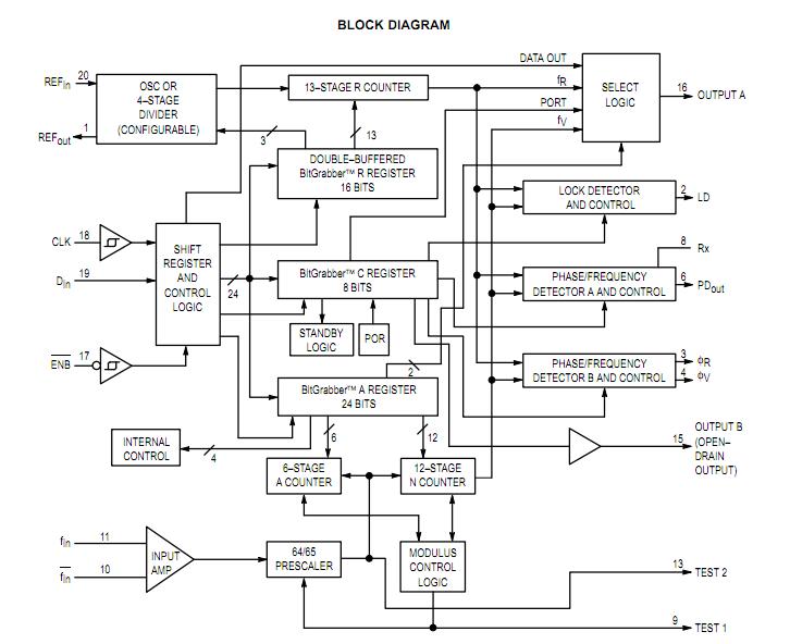
The MC145202F is a low–voltage single–package synthesizer with serial interface capable of direct usage up to 2.0 GHz. The counters are programmed via a synchronous serial port which is SPI compatible. The serial port is byte-oriented to facilitate control via an MCU. Due to the innovative BitGrabber Plus registers, the MC145202F may be cascaded with other peripherals featuring BitGrabber Plus without requiring leading dummy bits or address bits in the serial data stream. In addition, BitGrabber Plus peripherals may be cascaded with existing BitGrabber peripherals.
Parametrics
MC145202F absolute maximum ratings: (1)VCC, VDD DC Supply Voltage (Pins 12 and 14): – 0.5 to + 6.0 V; (2)VPD DC Supply Voltage (Pin 5): VDD – 0.5 to + 6.0 V; (3)Vin DC Input Voltage: – 0.5 to VDD + 0.5 V; (4)Vout DC Output Voltage (except OUTPUT B, PDout, φR, φV):– 0.5 to VDD + 0.5 V; (5)Vout DC Output Voltage (OUTPUT B, PDout, φR, φV): – 0.5 to VPD + 0.5 V; (6)Iin, IPD DC Input Current, per Pin (Includes VPD): ± 10 mA; (7)Iout DC Output Current, per Pin: ± 20 mA; (8)IDD DC Supply Current, VDD and GND Pins: ± 30 mA; (9)PD Power Dissipation, per Package: 300 mW; (10)Tstg Storage Temperature: – 65 to + 150℃; (11)TL Lead Temperature, 1 mm from Case for 10 Seconds: 260℃.
Features
MC145202F features: (1)Maximum Operating Frequency: 2000 MHz @ – 10 dBm; (2)Operating Supply Current: 4 mA Nominal at 3.0 V; (3)Operating Supply Voltage Range (VDD and VCC Pins): 2.7 to 5.5 V; (4)Operating Supply Voltage Range of Phase Detectors (VPD Pin): 2.7 to 5.5 V; (5)Current Source/Sink Phase Detector Output Capability: 1.7 mA @ 5.0 V 1.0 mA @ 3.0 V; (6)Gain of Current Source/Sink Phase/Frequency Detector Controllable via Serial Port; (7)Operating Temperature Range: – 40 to + 85°C; (8)R Counter Division Range: 1 and 5 to 8191; (9)Dual–Modulus Capability Provides Total Division up to 262,143; (10)High–Speed Serial Interface: 4 Mbps; (11)OUTPUT A Pin, When Configured as Data Out, Permits Cascading of Devices; (12)Two General–Purpose Digital Outputs — OUTPUT A: Totem–Pole (Push–Pull) with Four Output Modes OUTPUT B: Open–Drain; (13)Patented Power–Saving Standby Feature with Orderly Recovery for Minimizing Lock Times, Standby Current: 30 μA; (14)Evaluation Kit Available (Part Number MC145202EVK); (15)See Application Note AN1253/D for Low–Pass Filter Design, and AN1277/D for Offset Reference PLLs for Fine Resolution or Fast Hopping.
Diagrams
 |
 MC14000UB |
Other |
|
Data Sheet |
Negotiable |
|
||||||||||||||||
|
MC14001B |
Other |
|
Data Sheet |
Negotiable |
|
||||||||||||||||
|
MC14001BCP |
ON Semiconductor |
IC GATE NOR QUAD CMOS 14DIP |
Data Sheet |
|
|
||||||||||||||||
 |
MC14001BCPG |
ON Semiconductor |
Gates (AND / NAND / OR / NOR) 3-18V Quad 2-Input NOR |
Data Sheet |
|
|
||||||||||||||||
|
MC14001BDG |
ON Semiconductor |
Gates (AND / NAND / OR / NOR) 3-18V Quad 2-Input NOR |
Data Sheet |
|
|
||||||||||||||||
 |
MC14001BDR2 |
|
IC GATE NOR QUAD CMOS 14SOIC |
Data Sheet |
|
|
||||||||||||||||